We have actively designed and fabricated nanostructures, particularly plasmonic nanostructures, for biosensors and optoelectronic devices. We have developed a variety of nanofabrication techniques for integrating functional nanostructures into devices.
Nanofabrication for biosensing.
Biosensing with SERS is typically conducted with an optical microscope, so the nanopatterns cover areas of several tens to hundreds of square microns.
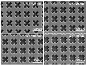
- We have used electron beam lithography and metal deposition to fabricate FDTD-designed quasi-3D nanopatterns, allowing us to conduct fundamental plasmonic studies and achieve sensitive and reproducible SERS detections.
- To make SERS-active substrates mass-producible, we fabricated silicon master modes and utilized soft lithography to transfer patterns into PDMS for either stand-alone SERS substrates or for integration into microfluidic channels.
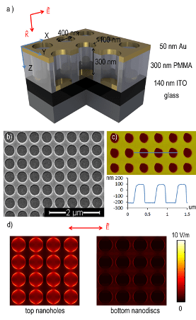
- To produce long-range SERS substrates, we applied and further developed solvent-assisted nanomolding method to form gold nanohole arrays on low-dielectric polymer layers.
Nanofabrication and processing for optoelectronic devices.
To fabricate plasmonic nanostructures for enhanced photovoltaic devices and photodetectors, a great challenge is found in making uniform nanostructures over a large area on different materials.
- For photovoltaic devices, we developed nanoimprinting method to make gold nanohole arrays on rigid glass, flexible PET and conformable Parylene substrates.
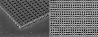
- For the UV photodetectors, we applied nanosphere lithography. This method not only produces large area nanopatterns cheaply and quickly, but also utilizes a mild organic solvent to remove the nanospheres and form desired aluminum nanohole arrays on glass substrates.
- We also combined nanosphere and soft lithography to make nanohemisphere patterns on the top of organic active layers and then transfer those patterns to the subsequent charge transport layer and electrode to produce plasmonic nanostructures in the top electrodes.


