Optoelectronic devices, such as solar cells and photodetectors, often adopt a device structure with multiple vertically stacked layers consisting of a light-absorbing active layer sandwiched by electron and hole transport layers, with an optically transparent front electrode and a metal back electrode. Over the years, we have focused on developing a variety of optoelectronic materials for applications in solar cells and photodetectors: organometal halide perovskites, semiconducting polymers, quantum dots, and nanocomposites of semiconducting polymers and quantum dots for the light-absorbing active layers; PEDOT:PSS derivatives and conductive transparent oxides for transparent hole-transport materials; and plasmonic nanostructures for transparent electrodes.
Tin-based organometal halide perovskite thin films.
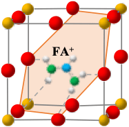
Organometal halide perovskites have emerged as promising new optoelectronic materials. The optoelectronic properties of perovskites can be widely tuned by varying their chemical compositions, which have a formula of AMX3, where A is a monovalent cation (e.g., methylammonium (MA+, CH3NH3+), formamidinium (FA+, CH3(NH2)2+), and/or cesium (Cs+)), M is a divalent transition metal cation (e.g., Pb2+ and/or Sn2+), and X is a halide anion (e.g., I-, Br-, and/or Cl-). To address the two major challenges for perovskite photovoltaics: lead toxicity and phase instability, we have focused primarily on tin-based perovskites with the goals to reduce toxicity and develop doping and passivation methods to suppress phase instability.
- We developed a solvent vapor assisted thermal annealing method that produces large, densely packed alloyed lead-tin perovskites by continual breaking and reforming of the tin-iodide bond mediated by solvent molecules.
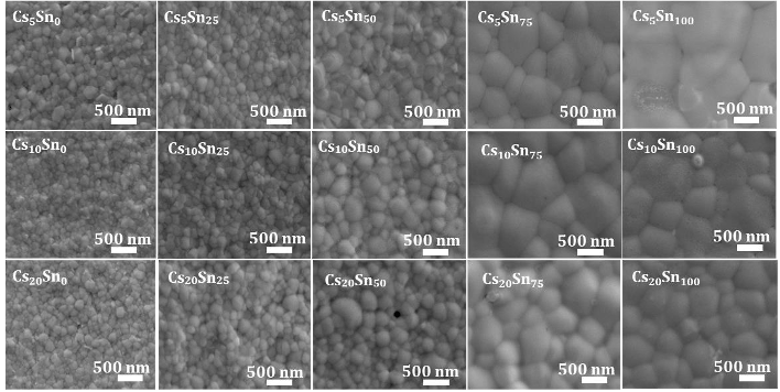
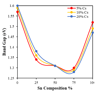
- To enhance the phase stability, we introduced inorganic cesium cations into the A-site to form triple cations (Cs/MA/FA) in the lead-tin double halides (I/Br) perovskites. We successfully made pure photoactive cubic-phase perovskites with metal compositions ranging from pure lead to pure tin. Integrating Cs+ greatly improved the phase stability and added variety to the structural and electronic properties, because it changed M-X bond overlapping and MX6 octahedral tilting.
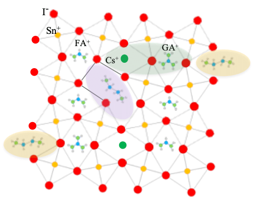
- We incorporated the ethylenediammonium diiodide (EDAI2) additive into a (CsGA)xFA 1-2xSnI 3+ y% EDAI2, which utilizes the strong hydrogen bonding of the guanidinium cation and the lattice strain relaxation of the small cesium cation as well as the hollowing and passivation effects of the EDAI2 additive. The EDAI2 additive not only yields pinhole-free cubic phase perovskite films but also decreases both shallow and deep trap states in the perovskite films.
Conducting polymers for hole transport materials.
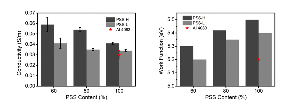
PEDOT:PSS has been widely used as a hole transport material in photovoltaic devices and photodetectors because of its solution processability, high transparency, and good flexibility. However, its relatively low conductivity and poor electron-blocking capability can be detrimental to the operational parameters of photovoltaic devices. We have therefore proposed to attach functional groups to the oxyethylene ring of EDOT, to modify the electrical conductivity and work function of the resulting polymers by varying the energy level of the highest occupied molecular orbital and the microstructure of polymer domains. In addition, the presence of functional groups on the hole transport layer surface could reduce interface defects in devices, improving overall charge transport.
- We have successfully synthesized EDOT monomers with hydroxymethyl (-MeOH) and chloromethyl (-MeCl) functional groups and have polymerized them into PEDOT-MeOH:PSS and PEDOT-MeCl:PSS using the oxidative chemical polymerization method.
- The subsequent process-structure-property studies not only provide us the means to modify PEDOT:PSS derivatives as hole transport materials but also shed light on the development of biocompatible conducting polymers for our ongoing OECT biosensing research and our emerging research on bioelectronics.
Semiconductor nanomaterials.
Semiconductor nanomaterials have unique optical and electronic properties. Our goal is to synthesize and grow new semiconductor nanomaterials with tunable properties. We implement a molecular level understanding of growth mechanisms to better control phase purity, morphology, and surface states of nanomaterials.
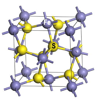
- We successfully synthesized pure pyrite FeS2 nanocrystals with controlled size and shape via orientated attachment and further enlarged the band gap via oxygen doping from a capping ligand.
- We synthesized a variety of semiconductor nanocrystals, such as CdSe quantum dots and nanorods, ZnO nanocrystals, and perovskite quantum dots, which forms nanocomposites by blending with semiconducting polymers.

