Optoelectronic devices such as solar cells, photodetectors, light emitting diodes (LEDs) and lasers have broad applications, from sustainable energy to missile detection to new lighting sources. Building on our understanding of plasmonic fundamentals and capabilities to grow controlled perovskites and synthesize new hole transport materials, we have aimed to make high performance photovoltaic devices and photodetectors by: (1) utilizing new and emerging semiconductor materials, (2) designing plasmonic nanostructures to enhance light absorption, and (3) designing device architectures to manipulate the charge transport processes.
Perovskite photovoltaic devices.
Perovskite photovoltaic devices typically adopt either the conventional n-i-p or inverted p-i-n structures, where n, i, and p represent the electron transport layer, perovskite layer, and hole transport layer, respectively. Although the record-high PCE values have been achieved by the conventional n-i-p structured perovskite solar cells, the inverted p-i-n structured perovskite solar cells have attracted more attentions recently because of their low-temperature (<150 ℃) solution processability, which makes them a great candidate for commercialization. Therefore, we have focused on the inverted p-i-n structured devices utilizing Sn-based and methylammonium (MA)-free perovskites and PEDOT:PSS-based hole transport layers.
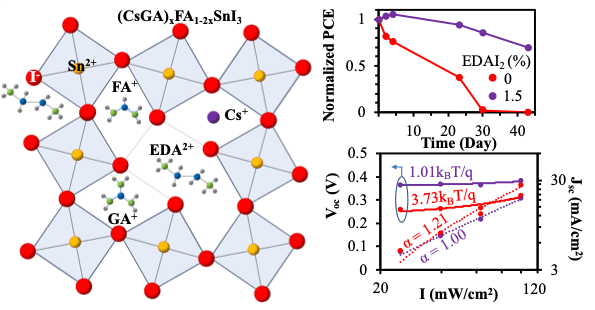
- We have manipulated the A-site cations to achieve stable Sn-based perovskite solar cells by introducing an inorganic cation, Cs+, into the perovskites of triple cations (Cs/MA/FA) lead-tin double halides (I/Br) and incorporating the ethylenediammonium diiodide (EDAI2) additive into a cesium–guanidinium doped formamidinium tin triiodide perovskites.
- We have fabricated MA-free perovskites to increase the intrinsic phase stability and further investigated the device instability induced by defect mediated ion migration under electric field.
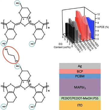
- We have developed new PEDOT:PSS derivatives and applied post-synthesis treatments to modify PEDOT:PSS electrical, structural, and surface properties to achieve better device performance by improving the energetic alignment and reducing trap states between the hole transport and active layers.
Organic solar cells.
Compared to their inorganic counterparts, organic materials tend to be cheaper, lighter, and more abundant, and they offer the added benefits of flexibility, solution processability, and tunable optoelectronic properties. Organic solar cells with the inverted structure have the advantages of better ambient stability and device processing. In inverted devices, it is important to prepare a selective bottom cathode to effectively reverse the device polarity from a conventional to an inverted structure and to make a top anode that can effectively transport holes while blocking electrons. We have focused on making electron and hole transport layers and developing plasmonic nanostructures as conductive, transparent electrode for flexible and conformable devices with the goal to make light, flexible solar cells for ubiquitous energy harvesting.
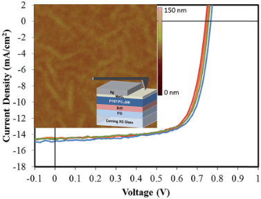
- We have fabricated the ZnO electron transport layer via sol-gel methods and investigated how polymer solar cell performance related to ZnO thin film morphologies.
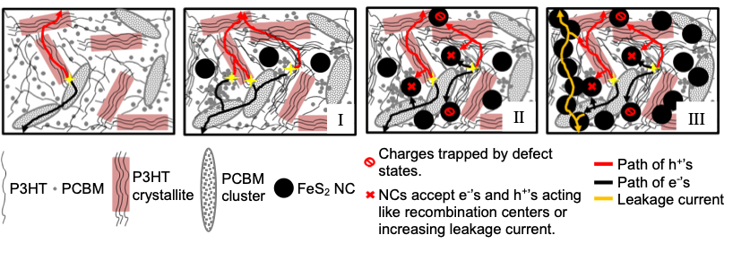
- We have made nanocomposite solar cells, containing P3HT with semiconductor FeS2 nanocrystals and PTB7 with CdSe quantum dots and nanorods, and investigated how microstructures of nanocomposites affect charge transport and device performance.
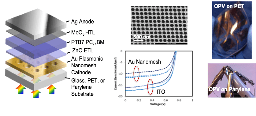
- We have integrated plasmonic nanohole arrays into organic solar cells as transparent conductive electrodes for the following benefits: (1) to replace indium tin oxide (ITO) to enable flexible, even conformable, devices, and (2) to tune and enhance light transmission to match the active layer band gap and absorption. We designed and fabricated plasmonic nanohole arrays as transparent electrodes for both inverted and conventional structured organic solar cells and achieved working devices on rigid glass, flexible PET, and conformable Parylene substrates.
Ultraviolet Photodetectors.
In general, photodetectors have a wide range of applications. For ultraviolet (UV) photodetectors, applications like environmental monitoring and laboratory instrumentation require a broadband UV response, while applications like filter-free imaging and colorimetry require a wavelength-specific narrowband response. It is therefore desirable to produce devices with a photoresponse that is not only strong, but also tunable and UV-selective. We have focused on designing photodiode-typed devices to achieve a low dark current, strong photoresponse, and tunable spectral selectivity using a variety of active layer materials including perovskites, organic semiconductors, and nanocomposites. We have also pioneered the integration of plasmonic nanostructures into photodetectors, both as a transparent bottom electrode or at the top of active layer, to enhance light absorption and charge transport and to manipulate spectral selectivity.
- We have produced densely packed, uniform thin films of methylammonium lead trichloride (MAPbCl3) using a two-step solvent vapor assisted thermal annealing method and demonstrated the UV-specific photodetection between ~290-420 nm under a low reverse bias.
- We have integrated aluminum nanohole arrays and nanohemisphere arrays into organic UV photodetectors as a transparent electrode and a top electrode, respectively, to provide UV-specific photoresponse enhancements.
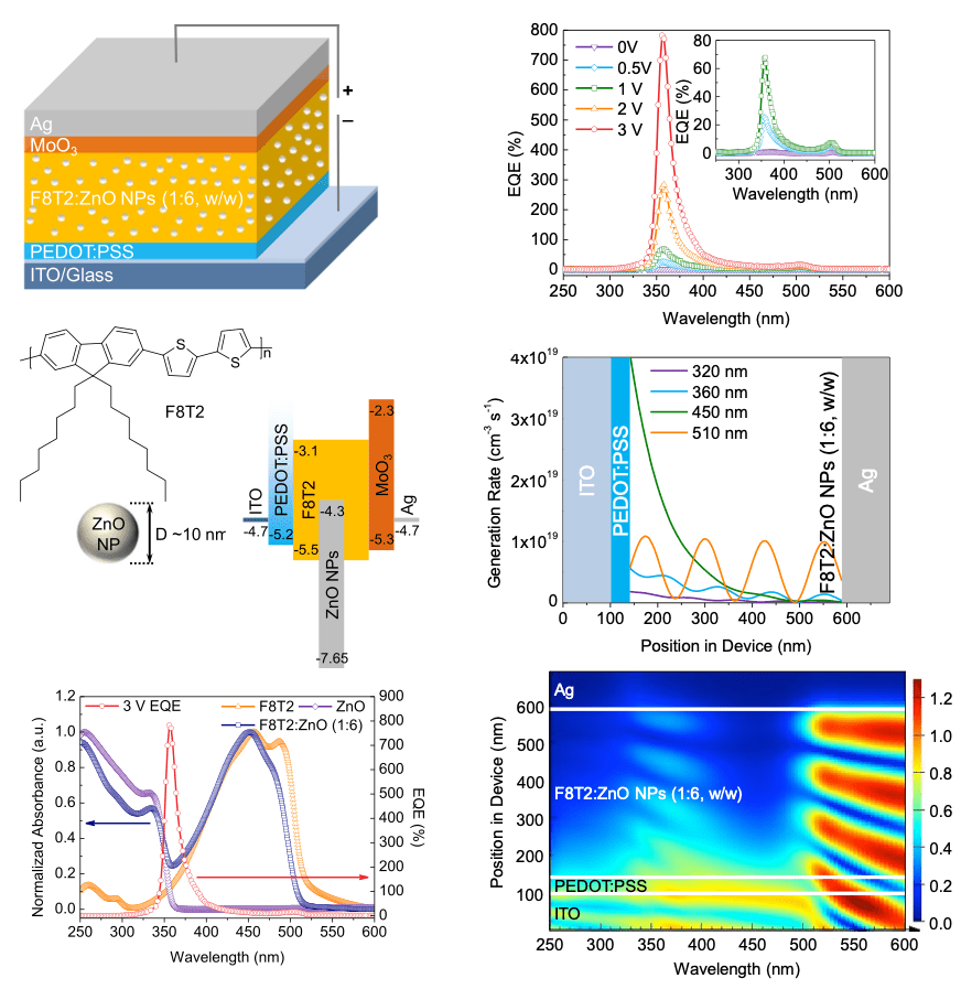
- We have mixed wide band gap ZnO nanoparticles with wide band gap conjugated polymers to achieve strong broadband and narrowband photoresponse under low biases. We applied finite-difference time-domain and transfer matrix method simulations to reveal the internal working mechanism and demonstrated that the nanocomposite active layer was stable in flexible photodetectors.
